Phosphorus is a vital component of every organism and plays a key role, for example, in energy transfer in the body and within cell membranes, bones and teeth. Phosphorus is also special because it occurs in numerous different forms (allotropes). For example, there is the highly explosive, toxic white phosphorus, the more stable red phosphorus known from match heads, or the crystalline, semi-conducting black phosphorus. The latter has numerous applications in electronic devices.
The variety of phosphorus compounds and their physical and chemical properties can be further extended by the self-assembly of two-dimensional phosphorus structures on surfaces.
Various two-dimensional layers
Researchers from a group led by Professor Ernst Meyer at the Department of Physics and the Swiss Nanoscience Institute at the University of Basel have now produced various two-dimensional phosphorus structures on silver surfaces by evaporating phosphorus atoms. The work is published in the journal Nature Communications.
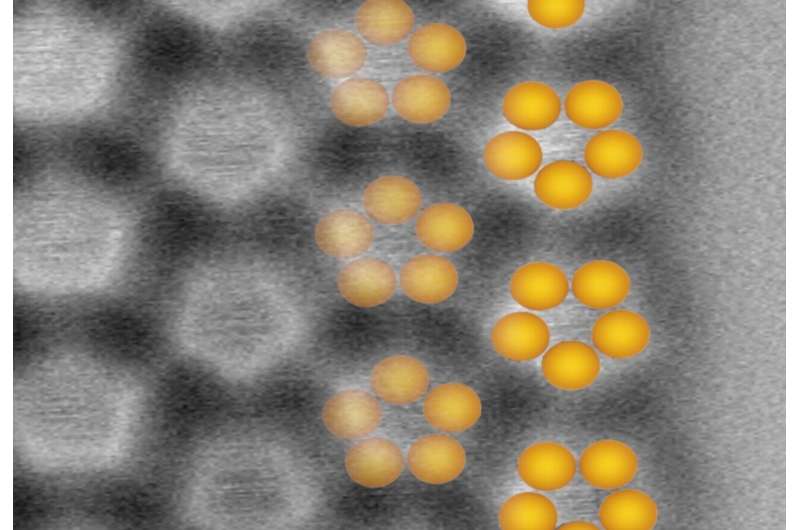
In addition to chains and hexagonal rings, they also produced planar rings of five phosphorus atoms (phosphorus pentamers), each of which behaves like an anion, i.e., is negatively charged.
In order to assess whether such 2D layers consisting of phosphorus pentamers are suitable for applications in nanoelectronics and nanooptics, it is necessary to characterize the properties of the atomic layer and investigate the interactions with the metallic surface.
Meaningful data through a combination of methods
Using a combination of atomic force and scanning tunneling spectroscopy at low temperatures of 4 kelvin (-269.15°C), the researchers found that the phosphorus pentamers retain their semiconducting properties on the silver surface.
“This distinguishes the phosphorus layer from a hexagonal graphene layer, for example, which is metallic when in direct contact with a metallic surface,” explains Dr. Rémy Pawlak, who supervised the experiments.
The phosphorus pentamer layer causes electrons to pass from the metal into the phosphorus layer and a special boundary layer, known as a p-type semiconductor-metal Schottky junction, is formed.
“The formation of a Schottky junction at the interface could enable applications in field-effect transistors, in solar cells or as diodes,” adds Professor Ernst Meyer.
The results were confirmed by simulations carried out by research groups from Shenzhen and Shanghai in China.
More information:
Outhmane Chahib et al, Probing charge redistribution at the interface of self-assembled cyclo-P5 pentamers on Ag(111), Nature Communications (2024). DOI: 10.1038/s41467-024-50862-4
Provided by
University of Basel
Citation:
2D layer of phosphorus pentamers shows semiconductor properties on silver surface (2024, August 9)
retrieved 9 August 2024
from https://phys.org/news/2024-08-2d-layer-phosphorus-pentamers-semiconductor.html
This document is subject to copyright. Apart from any fair dealing for the purpose of private study or research, no
part may be reproduced without the written permission. The content is provided for information purposes only.


