Similar to traditional semiconductors, lead halide perovskites achieve effective electrical doping

For traditional semiconductor materials and devices, controlling the distribution of electrical doping to build an internal electric field is a common method to enhance carrier extraction efficiency. Therefore, electrical doping is of great significance for the construction of high-performance devices.
In recent years, with the rapid improvement of device performance, organic-inorganic hybrid lead halide perovskite materials have become the most promising new type of semiconductor materials.
It is generally believed that lead halide perovskite is a bipolar semiconductor, making it difficult to realize electrical doping, and due to the large carrier diffusion length of perovskites, it is also generally believed that an internal electric field is not necessary for carrier collection. In addition, the measured carrier concentration of perovskites is generally on the order of 1013 to 1014 cm-3, which is not sufficient to form an effective electric field for carrier extraction.
To address the above issues, a collaboration has demonstrated through various characterization methods that molecular remote doping can control the charge type and concentration of lead halide perovskite thin films and prepare n-type low-dimensional structures on the surface of three-dimensional structures to form vertical heterojunctions to promote carrier collection, leading to perovskite stack solar cell efficiencies exceeding 27%.

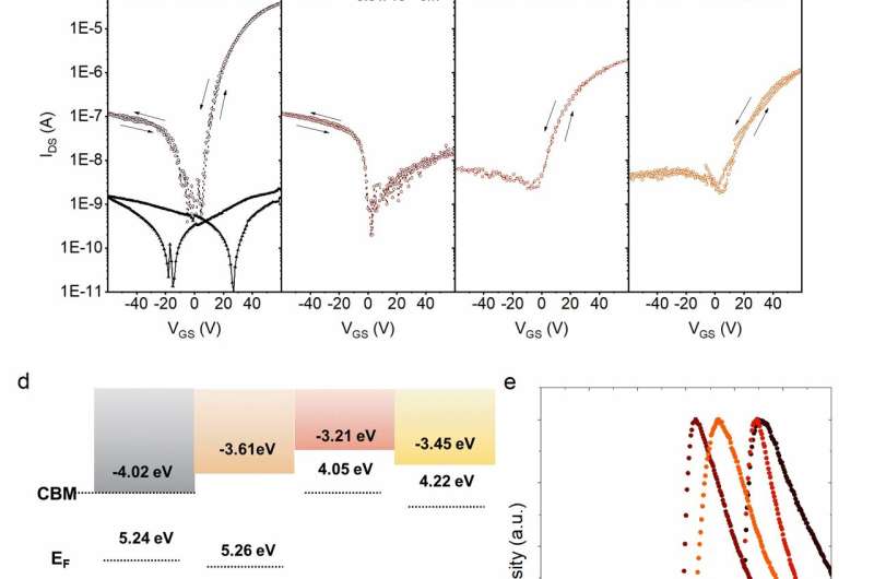
In order to accurately measure the electrical characteristics of perovskite, this work prepared a perovskite field effect transistor based on a cross-finger electrode array and conducted electrical testing using the pulse gate voltage method to suppress the hysteresis caused by ion migration, achieving accurate calibration of the doping concentration of lead halide perovskite.
Undoped films exhibit bipolar properties, films doped with ethylene diammonium molecules exhibit n-type properties, with a charge density close to the 1016 level, while films treated with benzyl ammonium exhibit p-type properties. Changes in film potential obtained by UV photoelectron spectroscopy and Kelvin probe testing are consistent with changes in electrical doping concentration, further confirming the remote molecular electrical doping on film.
In addition, doping with diammonium ions with similar structures can enhance surface potential (n-doping) as well, and continuous regulation of surface potential can be achieved by changing the concentration of ethylenediamine ions. These characterizations further confirm that diammonium ions can effectively electrically dope perovskite films.

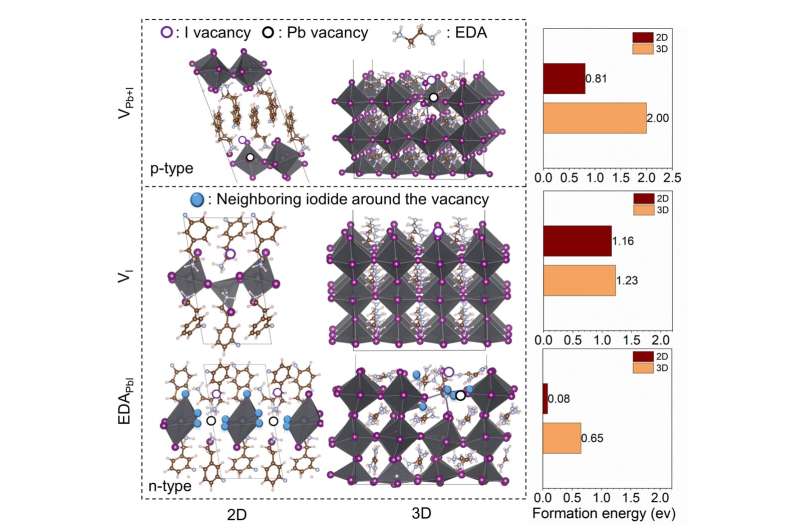
To understand the molecular doping mechanism, researchers used first-principles calculations to investigate the doping structure of the ethylenediamine ion, revealing that the ethylene diammonium cation can replace two neighbor ions of Pb+I, leading to n-type doping, while for the two-dimensional perovskite based on phenethyl ammonium, the formation energy of Pb+I vacancy defects is reduced, resulting in p-type doping. The multiple ion substitutions brought about by molecular doping provide an explanation for the electrical doping of thin films.
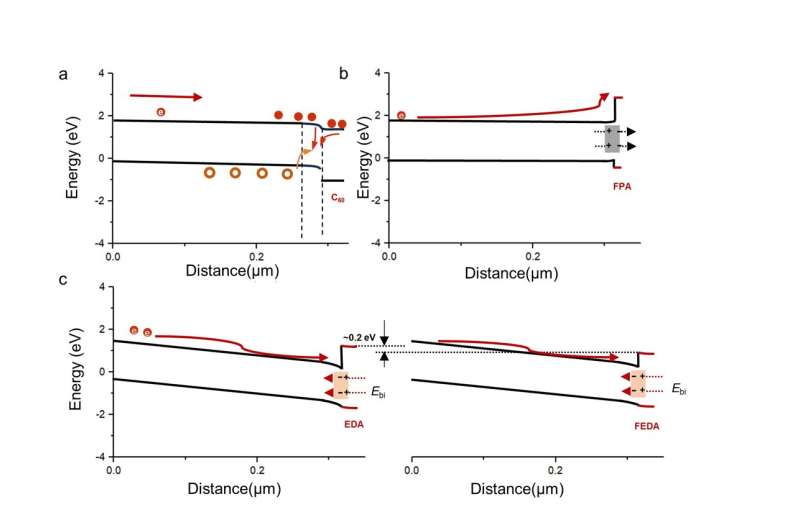
Based on the understanding of the electronic doping characteristics of perovskite, researchers further prepared n-type low-dimensional structures on the surface of a perovskite film through the co-doping of ethylene diammonium ions and phenethyl ammonium ions, forming a heterojunction with the underlying bipolar three-dimensional structure, reducing the interface electron transfer barrier and improving carrier extraction efficiency.
The transfer speed of carriers was characterized through transient absorption spectroscopy and transient photocurrent measurements, confirming that the formation of surface heterojunctions accelerates carrier extraction. In addition, the surface low-dimensional structure effectively passivates the perovskite surface, reducing the interface defects.

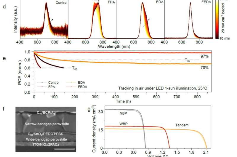
The use of three-dimensional to low-dimensional heterojunctions effectively enhances the current and voltage of inverted structure wide-bandgap perovskite solar cells, achieving a third-party certification efficiency of 19.3%. Additionally, the efficiency of tandem solar cells prepared by the combination of wide-bandgap and narrow-bandgap perovskites exceeds 27%.
This method has also been verified in normal bandgap perovskite cells, effectively improving device efficiency. Furthermore, the construction of surface heterojunctions accelerates carrier extraction, effectively reducing the accumulation of surface charges, suppressing ion migration in devices, and enhancing device stability.
The findings are published in the journal National Science Review.
More information:
Xianyuan Jiang et al, Surface heterojunction based on n-type low-dimensional perovskite film for highly efficient perovskite tandem solar cells, National Science Review (2024). DOI: 10.1093/nsr/nwae055
Citation:
Similar to traditional semiconductors, lead halide perovskites achieve effective electrical doping (2024, March 29)
retrieved 29 March 2024
from https://techxplore.com/news/2024-03-similar-traditional-semiconductors-halide-perovskites.html
This document is subject to copyright. Apart from any fair dealing for the purpose of private study or research, no
part may be reproduced without the written permission. The content is provided for information purposes only.


