[Adobe Stock]
Moore’s Law, which predicted the doubling of transistor density roughly every two years, is approaching fundamental physical limits. Yet, GPU technology continues to evolve rapidly, with innovations in architecture and specialized processing units driving consistent performance gains. Multi-chip modules, 3D chip stacking, and advanced cache hierarchies are pushing beyond monolithic die limitations. The first half of 2024 witnessed a wave of technological advances including the debut of Nvidia’s Blackwell GPU architecture, the widespread adoption of chiplet technology, and significant developments in thermal batteries and high-bandwidth memory. This feature examines some of the latest trends and breakthroughs in GPU and semiconductor technologies in the first half of 2024.
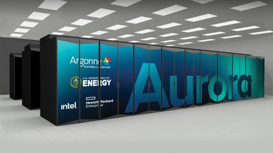
Aurora supercomputer achieves exascale performance, ranking second globally

[Wikipedia]
On May 13, 2024, Argonne National Laboratory announced at the ISC High Performance 2024 conference in Hamburg, Germany that the Aurora supercomputer surpassed the exascale barrier, achieving over a quintillion calculations per second. The Aurora is now the world’s second exascale machine, and is positioned in the second slot in the TOP500 ranking of supercomputers. The supercomputer’s scale and architecture, featuring 63,744 GPUs, could lead to potential advances in scientific research in areas ranging from climate change to medical treatments and materials science.
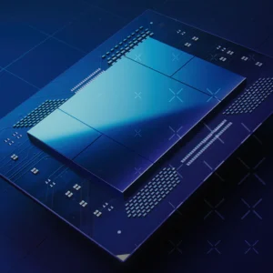
Chiplets making waves in semiconductor industry

[Arm]
In 2024, chiplet technology, where a single integrated circuit (IC) is composed of smaller, individual semiconductor dies, has attracted the attention of major players such as AMD, Intel, NVIDIA, and Samsung. The technology was also a star at the Design Automation Conference (DAC) 2024 event. MIT Technology Review recognized chiplets as one of the 10 Breakthrough Technologies for 2024 in Santa Clara. Interest in chiplets is not limited to the U.S. Chinese firms and government agencies, for instance, are investing heavily in chiplet R&D. Japan is as well, with companies like Tenstorrent licensing chiplet designs to the country’s Leading-edge Semiconductor Technology Center (LSTC).
Thermal batteries gaining ground for industrial energy storage and decarbonization applications
Thermal energy storage systems, also referred to as thermal batteries, hold promise for industrial energy management and decarbonization efforts. Such systems store energy as heat and can capture and retain large amounts of thermal energy over extended time frames. Companies like Rondo Energy, Antora Energy, and Electrified Thermal Solutions are developing such systems, storing energy in materials such as molten salt, concrete, engineered bricks, or carbon blocks.
Rondo Energy, for instance, uses bricks made from common materials to store heat at high temperatures. Its thermal batteries can deliver continuous, high-temperature heat up to 1500 degrees Celsius. This technology is in use at the 2 MWh heat battery installed at Calgren Renewable Fuels in California, which helps reduce the carbon intensity of biofuel production.
Antora Energy is taking a slightly different approach, using blocks of solid carbon to store heat. Its thermal batteries can convert renewable electricity into heat and then back into electricity via thermophotovoltaic cells. This dual capability allows for both direct industrial heat applications and electricity generation.
Finally, Electrified Thermal Solutions is focusing on using conductive bricks to store thermal energy, tapping the inherent advantages of thermal storage systems: high efficiency, low cost, and the ability to integrate with renewable energy sources.
Georgia Tech researchers create first functional graphene semiconductor
For decades, researchers have touted the promise of graphene. But the material has been hard to tap in semiconductor applications. But in January 2024, a team of scientists based in Atlanta, Georgia, and Tianjin, China, announced that they had created the world’s first functional semiconductor made entirely of graphene. The material offers 10 times greater mobility than silicon. The researchers did so by conquering the so-called “band gap” hurdle that previously held graphene back. The result? A material that could pave the way for faster, more efficient devices. This graphene-based semiconductor combines the exceptional conductivity of graphene with the crucial ability to switch on and off. That’s a property key to digital electronics. Potential applications could span from enabling smaller, faster electronic devices to quantum computing.
Nvidia unveils next-gen Blackwell GPU architecture

[NVIDIA]
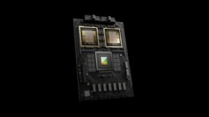
In March 2024, Nvidia debuted its Blackwell architecture at its GTC conference. The new architecture, set to power products like the B200 GPU and the GB200 Grace Blackwell Superchip, promises substantial performance gains over its predecessor, Hopper.
Nvidia targets a 4x increase in training performance at the cluster level compared to the H100 GPU. For specific inference workloads, particularly with large language models, Nvidia claims up to a 30x performance boost under certain conditions. Raw computing power sees a 2.5x improvement in standard formats, potentially reaching 5x when using the new FP4 format. One product embodying the new architecture is the B200 GPU, which features 208 billion transistors manufactured using TSMC’s 4NP process. Another example is the GB200 Grace Blackwell Superchip, which combines two B200 Tensor Core GPUs with the Nvidia Grace CPU, delivering significant performance gains for AI workloads. For instance, for a GPT-3 LLM benchmark with 175 billion parameters, the GB200 reportedly offers seven times the performance of an H100 GPU, as The Verge has noted.
Major cloud providers and tech companies, including AWS, Microsoft, Google, and Oracle, plan to adopt Blackwell-based systems.
HBM3E ushers in new era of memory bandwidth

[Samsung]
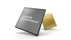
High Bandwidth Memory (HBM) is a computer memory interface designed for 3D-stacked synchronous dynamic random-access memory (SDRAM) that Samsung, AMD, and SK Hynix announced in 2013. In 2024, the High Bandwidth Memory (HBM) market saw significant improvements, especially in terms of High Bandwidth Memory 3E (HBM3E), the latest generation of the tech. The latest generation of high-performance memory is designed to help close the gap between the rapidly advancing processing capabilities of GPUs and growing memory bandwidth requirements. Examples of tangible developments include the SK Hynix, a 36GB memory product that began volume production in March 2024. It can achieve a data processing rate of up to 1.15TB per second. The company plans to mass-produce 12-layer HBM3E chips in the third quarter of 2024. SK Hynix has also developed a 16-layer 48GB HBM3E product that boasts a single-stack speed of up to 1280 GB/s. Meanwhile, Samsung Electronics also announced its HBM3E memory branded as “Shinebolt” (pictured).
Microsoft unveils $3.3 billion AI data center in Wisconsin, revitalizing stalled Foxconn site
On May 8 2024, Microsoft announced a potentially $3.3 billion investment in a Wisconsin AI data center on the site of the abandoned Foxconn project. The investment will cover cloud computing and AI infrastructure development, the creation of a manufacturing-focused AI co-innovation lab and AI skills training for more than 100,000 Wisconsin residents. The investment strategy has four main components. The first includes building a new datacenter campus in Mount Pleasant while the second encompasses establishing an AI Co-Innovation Lab at the University of Wisconsin-Milwaukee. The latter two goals include partnering with local organizations for AI skills training and investing in community education and youth employment programs. Microsoft expects the project to create 2,300 union construction jobs by 2025.


