
IITs, IISc roll out semiconductor courses. Army of engineers needed for India’s chip dream
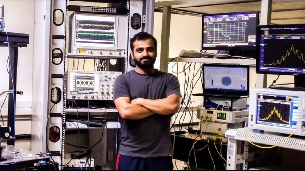
New Delhi: Professor Awanish Pandey’s new course on semiconductor technology at IIT-Delhi has filled all 70 seats in its very first run. And the students range from seasoned professionals at Intel to startup founders in Bengaluru.
“In the last two years, interest in semiconductor technology has skyrocketed,” said Pandey, an assistant professor at the Optics and Photonics Centre at the institute. “The India Semiconductor Mission has created a lot of awareness, in particular a focus on commercial manufacture.”
The India Semiconductor Mission (ISM), launched by the Ministry of Electronics and Information Technology in 2021, is India’s bid to become a domestic and global semiconductor powerhouse. Now, IISc Bengaluru, the IITs, and other top institutes are rapidly reorienting themselves to meet the surging demand for chips. They are rejigging their curricula, introducing new short-term courses, fine-tuning their PhD and MSc programmes, offering in-person training, and hosting online classes.
The goal is to train an army of engineers for an industry that India is betting heavily on, expected to reach $64 billion by 2026.
One thing is certain, the students who come to our courses want to make use of it. They enthusiastically ask us if they can start anything in the industry with Rs 10-15 lakh of capital
-Awanish Pandey, assistant professor at IIT-Delhi
Semiconductors form the backbone of modern technology, powering mobile phones, computers, AI systems, and even quantum machines. They’re also considered strategic assets in terms of national security. While Indians have long contributed to the design of chips for US-based companies like NVIDIA, there’s now a push toward manufacturing of semiconductors.
“Design is similar to how an architect creates blueprints for a building,” said Sushobhan Avasthi, a professor at the Centre for Nano Science and Engineering (CeNSE), Indian Institute of Science (IISc) in Bengaluru, Karnataka. “The architect is not involved in laying the foundation, building the walls, using the cement.”
It is to keep up with the growing interest in this foundational process that institutes across the country are rolling out new courses focused on fabrication.
Also Read: The next wars will be silent—fought with semiconductors, software, invisible lines of code
Fab training, faster
Chip tools, and fab labs aren’t just for PhDs anymore. IISc has launched a slew of short-term courses, ranging from two- and three-day workshops to one-month programmes, to cater to working professionals and students across learning levels.
“They vary from theoretical, online courses where just concepts are taught to more practical, in-person programmes where students get to experience the tools used in manufacturing,” said Avasthi. While these courses may not offer the depth of a PhD programme, they are certified under the National Skills Qualifications Framework (NSFQ). The prices range from a few thousand rupees to a little over a lakh.
In the 60-hour foundational course, delivered entirely online, students learn the basics of the fabrication, or ‘fab’, process—the multi-step manufacturing method that etches circuits onto silicon wafers.
Another 90-hour advanced course, run over two weeks, provides ‘eyes-on training’ to students, where they get to see the wafer being processed in person.
For students who want hands-on training, a deep-dive one-month course lets them begin working directly with the tools.
Other institutes are catching up as well. The New Age Makers’ Institute of Technology (NAMTECH), based at the IIT Gandhinagar campus in Gujarat, has launched a 12-month, in-person International Professional Master’s Program (iPMP) in semiconductor manufacturing. With a fee of nearly Rs 10 lakh, the course promises immersion opportunities in Germany and 100 per cent batch placement.
Last year, IIT-Delhi launched a six-month online executive programme targeting working professionals, priced at Rs 1.47 lakh. Divided into four modules, it covers the fundamentals, fabrication process, key equipment, and the latest developments by major players like NVIDIA and Intel.
“We get people from Intel, USA and Bosch, Germany in this course,” said Pandey proudly, adding that even employees from small startups in Bengaluru have signed up.
India already has enough engineers. We just need these bridge courses to upskill them
-Sushobhan Avasthi, professor at CeNSE, IISc
It’s far more specific than undergraduate programmes, which take a broader, more holistic approach.
“In our regular BTech courses, we make sure students know the A to Z of semiconductor technology, not just manufacturing,” Pandey added.
On the expense of in-person training, Avasthi said the real cost is often subsidised by the government, since semiconductor tools are capital intensive.
Despite the price tags, students see these courses as a stepping stone to future ventures.
“One thing is certain, the students who come to our courses want to make use of it,” Pandey said. “They enthusiastically ask us if they can start anything in the industry with Rs 10-15 lakh of capital.”
Also Read: How India is trying to win the semiconductor race, fighting decades of challenges & setbacks
Government chips in
Building a fabrication setup is no walk in the park. It takes precision tools, trained engineers, and heavy investment. In the last several years, the government has been putting serious money on the table, both in factories and training institutes.
One of its biggest investments far is in the country’s first commercial fab—the upcoming Tata Electronics semiconductor fabrication plant in Dholera, Gujarat, in partnership with Taiwan’s Powerchip Semiconductor Manufacturing Corporation (PSMC). The central government is covering 50 per cent of the Rs 90,000 crore cost, with the rest split between Tata and the Gujarat government.
Funding is also being channelled into research centres like CeNSE at IISc.
“The centre we run has received government investment of over Rs 300 crore over the last 14 years,” said Avasthi, pointing out that the amount is unusually large for an academic institution. “The government provides us with these semiconductor manufacturing tools through various research grants, with the expectation that we will run training programmes.”
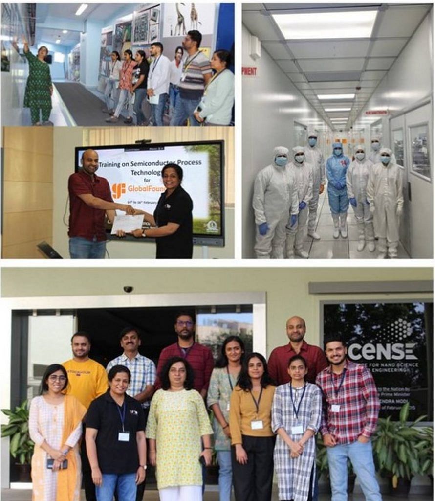
Because of this arrangement, IISc partners with several ministries to run its training programmes. A semiconductor fabrication course launched this year with the Ministry of Tribal Affairs is aimed at upskilling students from tribal communities. Another collaboration with the Ministry of Electronics, through the Indian National Users Portal (INUP), allows IISc to admit PhD and master’s students from other universities that lack semiconductor fabrication infrastructure.
But even as students’ interest in the field grows due to global headlines and the government’s push, work opportunities in fabrication are still limited.
While the Tata factory in Gujarat is expected generate 20,000 jobs—most requiring some level of expertise with semiconductors—it’s the only commercial fab currently in the pipeline.
“IISc has already trained the factory’s first 130 graduate engineering trainees, who are now deepening their knowledge in Taiwan,” said Avasthi.
Most students, however, can’t afford to wait for large-scale industry buildout. Their job needs are immediate and not everyone has the time or funds to pursue a multi-year research degree.
“India already has enough engineers,” said Avasthi, adding that supply of talent wasn’t the issue. “We just need these bridge courses to upskill them.”
(Edited by Asavari Singh)

")

