Samsung Marks Key Milestone with Tool-In Ceremony for $14.3B Semiconductor R&D Hub – Be Korea-savvy

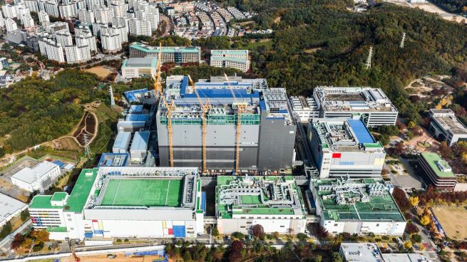
The ceremony marked the installation of the first batch of equipment at the NRD-K complex at its Giheung campus in Yongin, south of Seoul. (Image courtesy of Samsung Elecs)
SEOUL, Nov. 18 (Korea Bizwire) – Samsung Electronics Co., the world’s largest memory chipmaker, said Monday it held a tool-in ceremony for its new semiconductor research and development (R&D) complex near Seoul.
The ceremony marked the installation of the first batch of equipment at the NRD-K complex at its Giheung campus in Yongin, south of Seoul, signifying a key milestone in the transition from construction to manufacturing readiness.
NRD-K, which broke ground in 2022 in an area covering about 109,000 square meters, is designed as a comprehensive R&D hub for the company’s memory, system large scale integration and foundry semiconductor divisions.
The complex is expected to begin operations by mid-2025, with Samsung Electronics planning to invest a total of 20 trillion won (US$14.3 billion) in the facility by 2030.
NRD-K will be set up with cutting-edge production equipment, including high Numerical Aperture extreme ultraviolet lithography machines, which allow for finer and more precise chip patterning.
In addition, an advanced wafer bonding infrastructure is also planned to be installed.

This image provided by Samsung Electronics Co. shows its latest HBM3E 12H chips. (Image courtesy of Yonhap)
“NRD-K will bolster our development speed, enabling the company to create a virtuous cycle to accelerate fundamental research on next-generation technology and mass production,” Vice Chairman Hun Young-hyun said during the ceremony.
“We will lay the foundation for a new leap forward in Giheung, where Samsung Electronics’ 50-year history of semiconductors began, and create a new future for the next 100 years.”
Samsung Electronics’ Giheung campus is known as the birthplace of the world’s first 64-megabit DRAM in 1992, marking the beginning of the company’s leadership in the global semiconductor industry.
The company said through the establishment of the new R&D facility, it will foster the complex as a hub for semiconductor ecology and technological innovation.
(Yonhap)


